(China (Mainland))


Product Summary
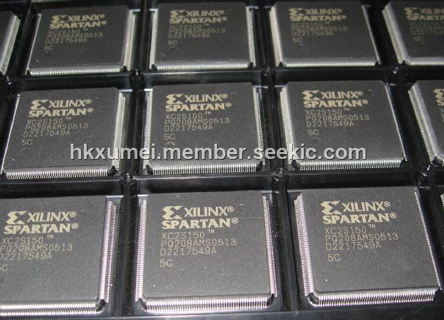
The XC2S150-5PQ208C is a Field-Programmable Gate Array. It gives users high performance, abundant logic resources, and a rich feature set, all at an exceptionally low price. The XC2S150-5PQ208C offers densities ranging from 15,000 to 200,000 system gates. System performance is supported up to 200 MHz. Features of the XC2S150-5PQ208C include block RAM (to 56K bits), distributed RAM (to 75,264 bits), 16 selectable I/O standards, and four DLLs. Fast, predictable interconnect means that successive design iterations continue to meet timing requirements. The XC2S150-5PQ208C is a superior alternative to mask-programmed ASICs. The XC2S150-5PQ208C FPGA avoids the initial cost, lengthy development cycles, and inherent risk of conventional ASICs. Also, FPGA programmability permits design upgrades in the field with no hardware replacement necessary (impossible with ASICs).
Parametrics
XC2S150-5PQ208C absolute maximum ratings: (1)VCCINT, Supply voltage relative to GND: –0.5 to 3.0 V; (2)VCCO, Supply voltage relative to GND: –0.5 to 4.0 V; (3)VREF, Input reference voltage: –0.5 to 3.6 V; (4)VIN, Input voltage relative to GND: -0.5 to 5.5V when 5V tolerant I/O; –0.5 to VCCO+0.5 V when No 5V tolerance; (5)VTS, Voltage applied to 3-state output:-0.5 to 5.5V when 5V tolerant I/O; –0.5 VCCO+0.5 V when No 5V tolerance; (6)TSTG, Storage temperature (ambient) –65 to +150℃; (7)TJ, Junction temperature +125℃ max.
Features
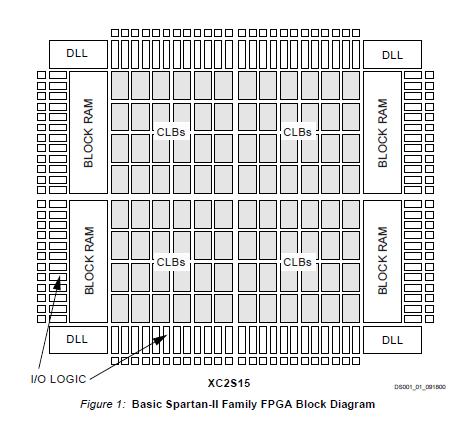
XC2S150-5PQ208C features: (1)Densities as high as 5,292 logic cells with up to 200,000 system gates; (2)streamlined features based on Virtex FPGA architecture; (3)Unlimited reprogrammability; (4)Very low cost; (5)Cost-effective 0.18 micron process; (6)Fully PCI compliant; (7)Low-power segmented routing architecture; (8)Full readback ability for verification/observability; (9)Dedicated carry logic for high-speed arithmetic; (10)Efficient multiplier support; (11)Cascade chain for wide-input functions; (12)Abundant registers/latches with enable, set, reset; (13)Four dedicated DLLs for advanced clock control; (14)Four primary low-skew global clock distribution nets; (15)IEEE 1149.1 compatible boundary scan logic.
Diagrams
| Image | Part No | Mfg | Description |  |
Pricing (USD) |
Quantity | ||||||
|---|---|---|---|---|---|---|---|---|---|---|---|---|
 |
 XC2S150-5PQ208C |
|
IC FPGA 2.5V 864 CLB'S 208-PQFP |
Data Sheet |
|
|
||||||
| Image | Part No | Mfg | Description | |
Pricing (USD) |
Quantity | ||||||
 |
XC2S100 |
Other |
|
Data Sheet |
Negotiable |
|
||||||
|
XC2S100-5FG256C |
|
IC FPGA 2.5V 600 CLB'S 256-FBGA |
Data Sheet |
|
|
||||||
|
XC2S100-5FG256I |
|
IC FPGA 2.5V I-TEMP 256-FBGA |
Data Sheet |
|
|
||||||
|
XC2S100-5FG456C |
|
IC FPGA 2.5V 600 CLB'S 456-FBGA |
Data Sheet |
|
|
||||||
|
XC2S100-5FG456I |
|
IC FPGA 2.5V I-TEMP 456-FBGA |
Data Sheet |
Negotiable |
|
||||||
|
XC2S100-5FGG256C |
|
IC SPARTAN-II FPGA 100K 256-FBGA |
Data Sheet |
|
|
||||||