(China (Mainland))

Product Summary
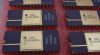
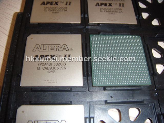
The EP2A40F1020I8 device integrates high-speed differential I/O support using the True-LVDS interface. The dedicated serializer, deserializer, and CDS circuitry in the True-LVDS interface support the LVDS, LVPECL, HyperTransport, and PCML I/O standards. Flexible-LVDS pins located in regular user I/O banks offer additional differential support, increasing the total device bandwidth. This circuitry, together with enhanced IOEs and support for numerous I/O standards, allows APEX II devices to meet high-speed interface requirements.
Parametrics
Absolute maximum ratings: (1)Maximum gates: 3,000,000; (2)Typical gates: 1,500,000; (3)LEs: 38,400; (4)RAM ESBs: 160; (5)Maximum RAM bits: 655,360; (6)True-LVDS channels: 36 (1); (7)Flexible-LVDSTM channels : 88; (8)True-LVDS PLLs: 4; (9)General-purpose PLL outputs: 8; (10)Maximum user I/O pins: 735.
Features
Features: (1)Programmable logic device (PLD) manufactured using a 0.15-μm alllayer copper-metal fabrication process (up to eight layers of metal): 1-gigabit per second (Gbps) True-LVDSTM, LVPECL, pseudo; (2)High-density architecture: 1,900,000 to 5,250,000 maximum system gates, Up to 67,200 logic elements (LEs), Up to 1,146,880 RAM bits that can be used without reducing; (3)available logic; (4)Low-power operation design: 1.5-V supply voltage, Copper interconnect reduces power consumption, MultiVoltTM I/O support for 1.5-V, 1.8-V, 2.5-V, and 3.3-V; (5)interfaces, ESBs offer programmable power-saving mode.
Diagrams
 |
 EP2A25F672C9 |
Other |
|
Data Sheet |
Negotiable |
|
||||||
|
EP2AGX125DF25C4 |
|
IC ARRIA II GX FPGA 125K 572FBGA |
Data Sheet |
|
|
||||||
 |
EP2AGX125DF25C4N |
|
IC ARRIA II GX FPGA 125K 572FBGA |
Data Sheet |
|
|
||||||
|
EP2AGX125DF25C5 |
|
IC ARRIA II GX FPGA 125K 572FBGA |
Data Sheet |
|
|
||||||
|
EP2AGX125DF25C5N |
|
IC ARRIA II GX FPGA 125K 572FBGA |
Data Sheet |
|
|
||||||
|
EP2AGX125DF25C6 |
|
IC ARRIA II GX FPGA 125K 572FBGA |
Data Sheet |
|
|
||||||