(China (Mainland))


Product Summary
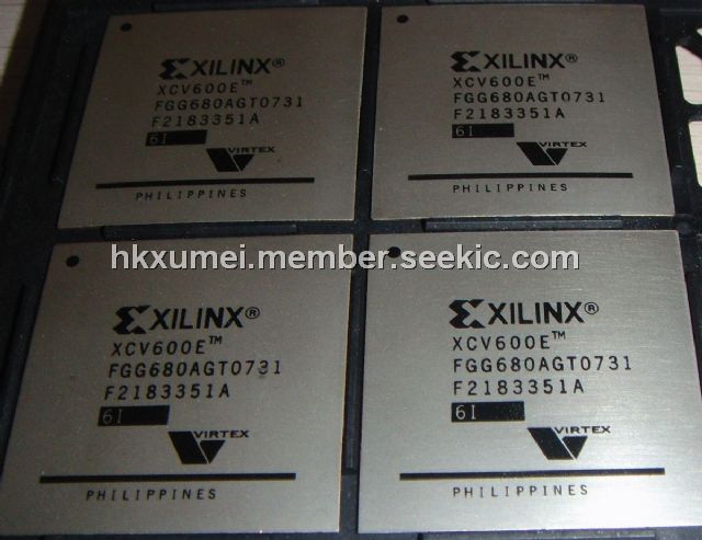
The XCV600E-6FGG680I is a Field-Programmable Gate Array (FPGA). The deivce gives users high performance, abundant logic resources, and a rich feature set, all at an exceptionally low price. The XCV600E-6FGG680I offers densities ranging from 15,000 to 200,000 system gates. System performance is supported up to 200 MHz. Features of the XCV600E-6FGG680I include block RAM (to 56K bits), distributed RAM (to 75,264 bits), 16 selectable I/O standards, and four DLLs. Fast, predictable interconnect means that successive design iterations continue to meet timing requirements. The XCV600E-6FGG680I is a superior alternative to mask-programmed ASICs. The FPGA avoids the initial cost, lengthy development cycles, and inherent risk of conventional ASICs. Also, the XCV600E-6FGG680I permits design upgrades in the field with no hardware replacement necessary (impossible with ASICs).
Parametrics
XCV600E-6FGG680I absolute maximum ratings: (1)VCCINT, Supply voltage relative to GND: –0.5 to 3.0 V; (2)VCCO, Supply voltage relative to GND: –0.5 to 4.0 V; (3)VREF, Input reference voltage: –0.5 to 3.6 V; (4)VIN, Input voltage relative to GND, 5V tolerant I/O: –0.5 to 5.5 V; No 5V tolerance: –0.5 to VCCO+0.5 V; (5)VTS, Voltage applied to 3-state output 5V tolerant I/O: –0.5 to 5.5 V; No 5V tolerance: –0.5 to VCCO+0.5 V; (6)TSTG, Storage temperature (ambient): –65 to +150℃; (7)TJ Junction temperature: +125℃ max.
Features
XCV600E-6FGG680I features: (1)Fully PCI compliant; (2)Low-power segmented routing architecture; (3)Full readback ability for verification/observability; (4)Dedicated carry logic for high-speed arithmetic; (5)Efficient multiplier support; (6)Cascade chain for wide-input functions; (7)Abundant registers/latches with enable, set, reset; (8)Four dedicated DLLs for advanced clock control; (9)Four primary low-skew global clock distribution nets; (10)Pb-free package options; (11)Low-cost packages available in all densities; (12)Family footprint compatibility in common packages; (13)16 high-performance interface standards; (14)Hot swap Compact PCI friendly; (15)Zero hold time simplifies system timing.
Diagrams
 |
 XCV600-4BG432C |
|
IC FPGA 2.5V C-TEMP 432-MBGA |
Data Sheet |
Negotiable |
|
||||
|
XCV600-4BG432I |
|
IC FPGA 2.5V I-TEMP 432-MBGA |
Data Sheet |
Negotiable |
|
||||
|
XCV600-4BG560C |
|
IC FPGA 2.5V C-TEMP 560-MBGA |
Data Sheet |
Negotiable |
|
||||
|
XCV600-4BG560I |
|
IC FPGA 2.5V I-TEMP 560-MBGA |
Data Sheet |
Negotiable |
|
||||
 |
XCV600-4FG676C |
|
IC FPGA 2.5V C-TEMP 676-FBGA |
Data Sheet |
Negotiable |
|
||||
|
XCV600-4FG676I |
|
IC FPGA 2.5V I-TEMP 676-FBGA |
Data Sheet |
Negotiable |
|
||||